Assertion (A) : Putting p type semiconductor slab directly in physical contact with n type semiconductor slab cannot form the pn junction.
Reason (R) : The roughness at contact will be much more than inter atomic crystal spacing and continuous flow of charge carriers is not possible
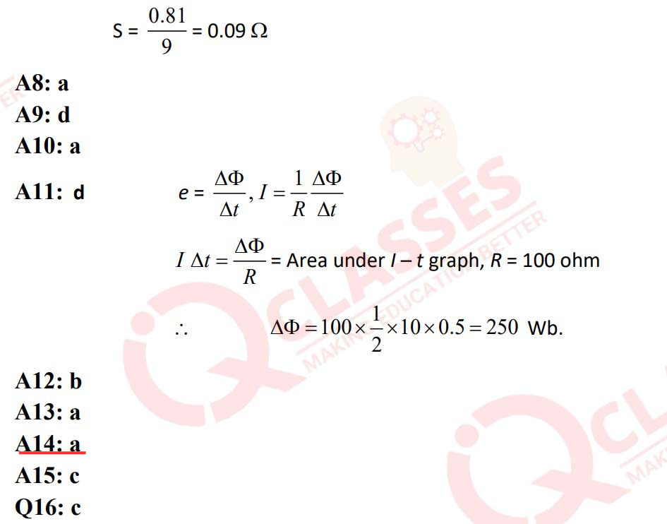
Solution