Class 12 CBSE Physics Semiconductor Electronics Boards Questions
Here we provide Class 12 physics important notes,board questions and predicted questions with Answers for chapter Semiconductor Electronics. These important notes,board questions and predicted questions are based on CBSE board curriculum and correspond to the most recent Class 12 physics syllabus. By practising these Class 12 materials, students will be able to quickly review all of the ideas covered in the chapter and prepare for the Class 12 Board examinations.
Class 12 CBSE Semiconductor Electronics Boards Questions
Semiconductor Electronics Boards Questions
2017
Q1
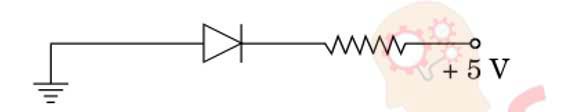
(a) In the following diagram, is the junction diode forward biased or reverse biased ?
(b) Draw the circuit diagram of a full wave rectifier and state how it works.
solutions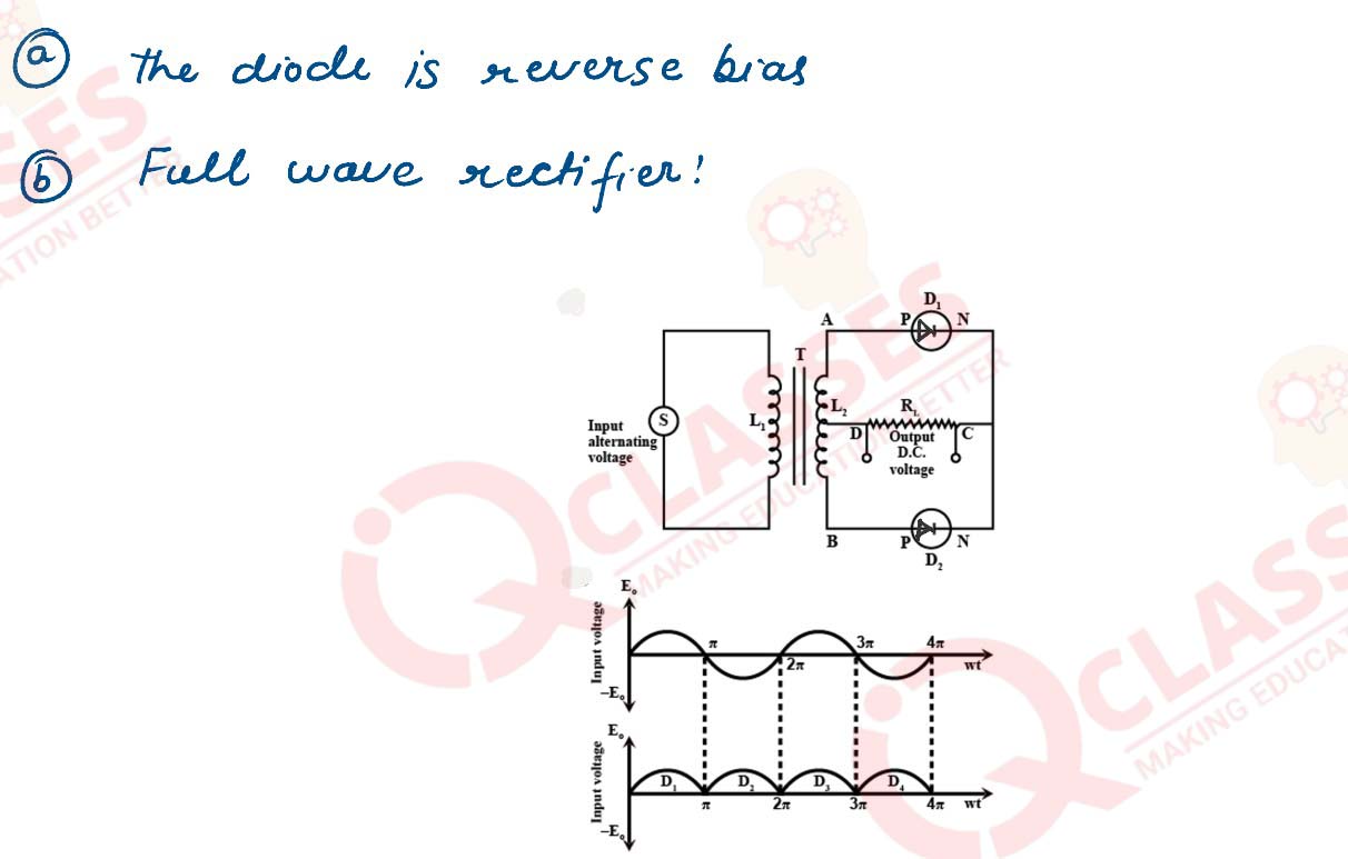
(b) Draw the circuit diagram of a full wave rectifier and state how it works.
solutions
2019
Q2
Three photo diodes D1, D2 and D3 are made of semiconductors having band gaps of 2.5 eV, 2 eV and 3
eV respectively. Which of them will not be able to detect light or vibrant 600 nm
solutions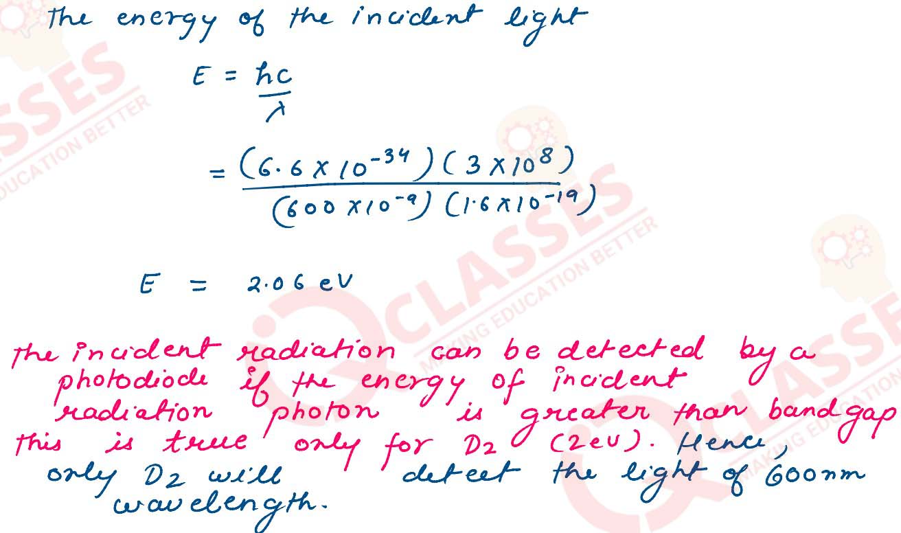
solutions
Q3
Why photo diodes are required to operate in reverse bias? Explain
solutions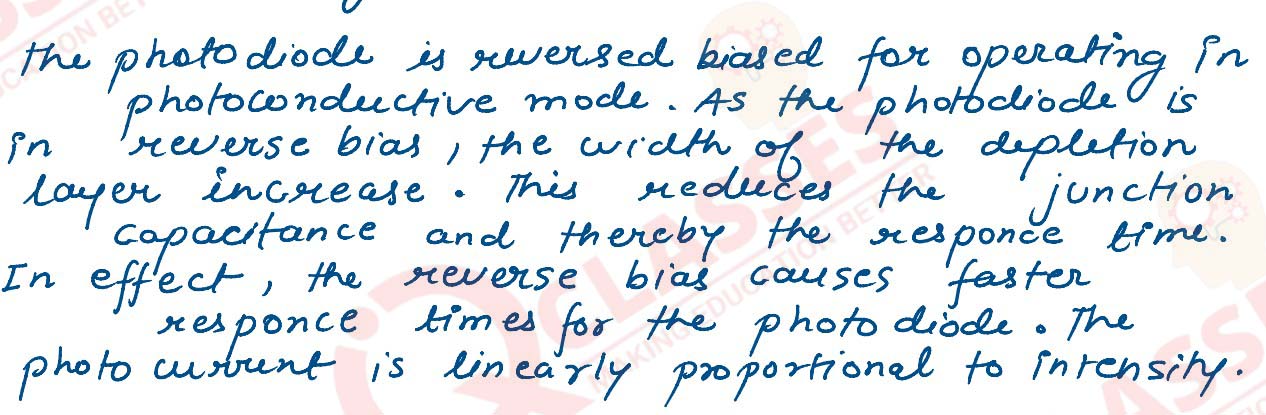
solutions
Q4
Draw the circuit diagram of full wave rectifier and explain its working also give the input and
output waveforms
solutions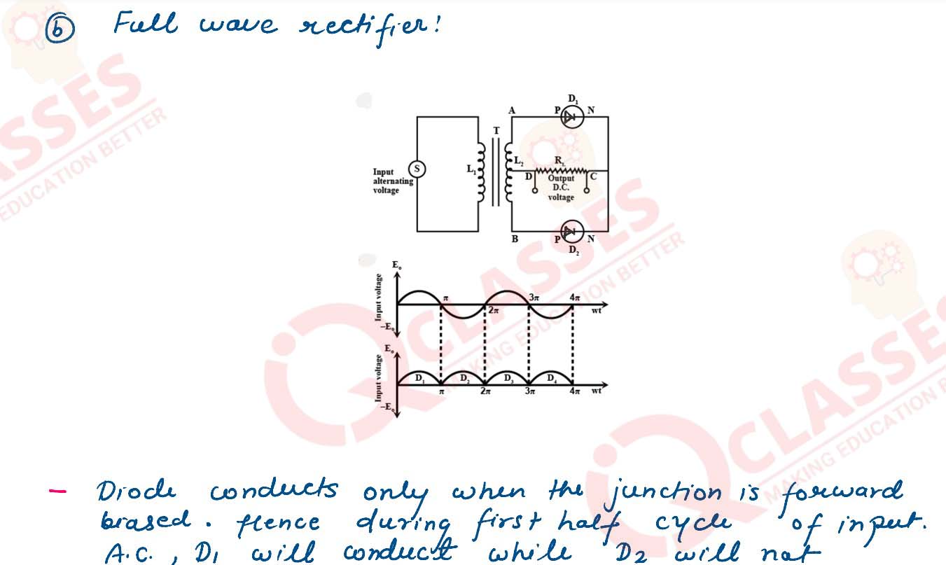

solutions
2020
Q5
How does an increase in doping concentration affect the width of depletion layer of a p-n junction
diode ?
solutions
solutions
Q6
Why cannot we use Si and Ge in fabrication of visible LEDs ?
solutions
solutions
Q7
Explain the terms ‘depletion layer’ and ‘potential barrier’ in a p-n junction diode. How are the (a)
width of depletion layer, and (b) value of potential barrier affected when the p-n junction is
forward biased ?
solutions
solutions
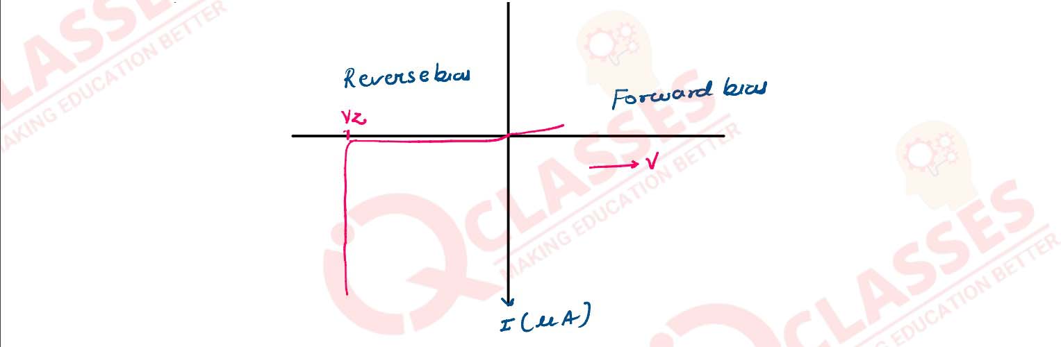
Q8
(a) Draw circuit diagram and explain the working of a zener diode as a dc voltage regulator with the
help of its I-V characteristic.
(b) What is the purpose of heavy doping of p- and n-sides of a zener diode ?
solutions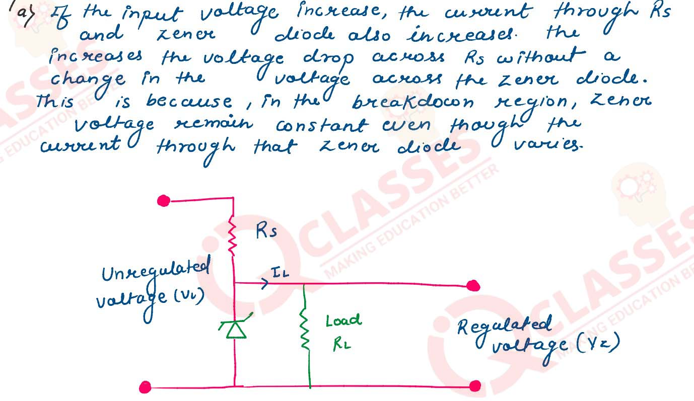

(b) What is the purpose of heavy doping of p- and n-sides of a zener diode ?
solutions


Reach Us
SERVICES
- ACADEMIC
- ON-LINE PREPARATION
- FOUNDATION & CRASH COURSES
CONTACT
B-54, Krishna Bhawan, Parag Narain Road,
Near Butler Palace Colony Lucknow
Contact:+918081967119
Add a comment